Input characteristics of common collector configuration Input characteristics are the relationship between the input current and input voltage keeping output voltage constant. Here input current is IB and input voltage VBE and output voltage is VCE. The output voltage VCE initially kept at 3V and kept constant. In this configuration, input current or base current is denoted by IB and output current or emitter current is denoted by IE.The common collector amplifier has high input impedance and low output impedance. It has low voltage gain and high current gain. The power gain of the common collector amplifier is medium.

Common Collector Configuration Circuit Diagram
Definition: The configuration in which the collector is common between emitter and base is known as CC configuration. In CC configuration, the input circuit is connected between emitter and base and the output is taken from the collector and emitter. Input Characteristics: The curve describes the changes in the values of input current with respect to the values of input voltage, keeping the output voltage constant. Output Characteristics: The curve is obtained by plotting the output current against output voltage, keeping the input current constant. The common collector or grounded collector configuration is generally used where a high impedance input source needs to be connected to a low impedance output load requiring a high current gain. Consider the common collector amplifier circuit below. Common Collector Amplifier using an NPN Transistor Definition: The configuration in which the emitter is connected between the collector and base is known as a common emitter configuration. The input circuit is connected between emitter and base, and the output circuit is taken from the collector and emitter.

Common Collector Configuration Input characteristics Multisim Live
A common collector amplifier using two-supply emitter bias is shown in Figure 7.4.1 7.4. 1. The input is coupled into the base like the common emitter amplifier, however, the output signal is taken at the emitter instead of at the collector. Because the collector is at the AC common, there is no need for a collector resistor. Common Base Configuration Input Characteristics Output Characteristics Common Collector Configuration Input Characteristics Output Characteristics Common Emitter Configuration Input Characteristics Output Characteristics output characteristics common emitter configuration. Input Characteristics common emitter configuration The graphs showing the variation of base current IB (input) with the variation of emitter-base voltage ( VEB) at a constant collector-emitter voltage ( VCE) are called input characteristics. In this video, the common collector configuration of the BJT (input and output characteristics ) has been explained briefly.By watching this video, you will.

Common collector configuration input and output characteristics of common collector transistor
Fig: Input and Output Characteristics of Common Collector Configuration. Output Characteristics: The output characteristics shown in Figure, are the same as those of the common emitter configuration. This characteristics shows the relation between the emitter current \(I_E\) and collector voltage \(V_{CE}\), for various fixed values of \(I_B\). 1 Kathi, it helps to realize that the signal voltage Vbc (between base and collector) is identical to the signal voltage Vbo (between base and common ground). This is because the internal ac resistance of the DC voltage source (connected to C) can be regarded as zero.
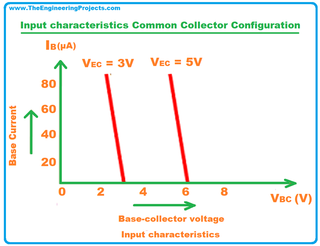
Sometimes common base configuration is referred to as common base amplifier, CB amplifier, or CB configuration. The input signal is applied between the emitter and base terminals while the corresponding output signal is taken across the collector and base terminals. Thus the base terminal of a transistor is common for both input and output. Input Characteristics: The input characteristics of a common collector configuration are quite different from the common base and common emitter configurations because the input voltage V BC is largely determined by V EC level.
BJT Definition, Symbol, Working, Characteristics, Types & Applications The Engineering Projects
For the common collector configuration, the output characteristics are a plot of IE versus VEC for a range of values of IB.The input current, therefore, is the same for both the common emitter and common collector characteristics. INPUT CHARACTERISTICS OF COMMON COLLECTOR CONNECTIONIn this circuit base of the transistor serves as input and emitter is the output and collector is common.
